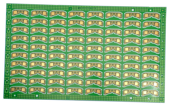
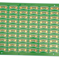
What is a double-sided PCB?
A double-layer PCB board with copper and metalized holes on both sides is called a double-layer board. Both sides of the circuit board are covered with circuit boards. However, if you want to use wires on both sides, you should first provide appropriate circuit connections between the two sides. Nowadays, double-sided printed circuit board technology remains the mainstay of the assembly industry. New and old designs have almost unlimited applications.
[email protected]
What materials are used to manufacture double-sided PCBs?
The core material is usually a glass fiber reinforced epoxy resin laminated board (FR4 is the most common), with copper foil bonded to each side. According to the requirements of the application, other materials may include polyimide, CEM1, and CEM3.
Application of double-sided PCB board
Industrial control
power supply
Consumer electronics
LED lighting
car
telephone system
Control relay
hard drive
Single sided printed circuit board and double-sided printed circuit board
The difference between a double-sided PCB board and a single-sided PCB board is that the single-sided PCB circuit is only located on one side of the PCB board, while the double-sided PCB circuit can be distributed on both sides of the PCB board. The wiring of the double-sided PCB board is currently being connected.
In addition to the different production processes of double-sided PCB boards and single-sided PCB boards, there is an additional copper deposition process, which is the process of conducting double-sided circuits.
Is double-sided PCB more expensive than single-sided PCB?
Generally speaking, yes. The manufacturing process of double-sided PCBs is more complex, involving additional steps such as through-hole electroplating. Compared to single-sided PCBs, this complexity may result in higher costs.
Can double-sided PCBs be used for high-frequency applications?
Yes, double-sided PCBs can be used for high-frequency applications. The key lies in the accuracy of the materials and layout used for the PCB substrate. High frequency PCBs typically require materials with low dielectric loss and designs that minimize signal interference, which can be achieved through careful planning and expertise in double-sided PCB design.
The advantages of double-sided PCB
A double-sided PCB makes it relatively easy to add conductive paths on the board, which means you will have a PCB that is more suitable for your needs;
Due to the fact that both sides of the double-sided PCB board are conductive, a large number of ICs and components can be assembled at any time;
If necessary, the size of the circuit board can be reduced as double-sided PCBs can be used, which may save you money as you may only need to use one board;
Double sided PCBs can be used for many different applications and electronic products, making them an ideal choice for demanding applications and advanced electronic products.
How to solder double-sided PCB
In order to ensure the reliable conductivity of double-sided printed circuit boards, it is necessary to first solder the connection holes (i.e. the through-hole part of the metallization process) on the double-sided printed circuit board with wires, and cut the protruding part of the connection wire tip to avoid injuring the operator's hand. This is the preparation work for wiring the circuit board.
Welding points for double-sided circuit boards:
For equipment that needs to be molded, it should be processed according to the requirements of the process drawings; That is to say, they must be molded first and then inserted.
After molding, the model side of the diode should face upwards, and there should be no difference in the length of the two pins.
When inserting devices with polarity requirements, be careful not to reverse their polarity. Rolling the integrated block components, after insertion, whether it is a vertical or horizontal device, there must be no obvious tilt.
The power of the soldering iron used for welding is between 25 and 40 watts. The temperature of the soldering iron tip should be controlled at around 242 ℃. If the temperature is too high, the tip is prone to "death", and if the temperature is low, the solder cannot melt. The welding time should be controlled within 3-4 seconds.
During formal welding, the operation is generally carried out from short to high and from inside to outside according to the welding principle of the equipment. Master the welding time. If the time is too long, the equipment will be burned out, and the copper wire on the copper-clad board will also be burned out.
Due to the double-sided welding, a process frame for placing the circuit board should also be made to avoid squeezing the components below.
After the circuit board is soldered, a comprehensive inspection should be conducted to identify areas of missing insertion and soldering. After confirming the correctness, trim the redundant device pins on the circuit board, and then proceed to the next process.
In specific operations, relevant process standards should be strictly followed to ensure the welding quality of the product.
How to reflow double-sided PCB
At present, the mainstream circuit board assembly technology in the SMT industry should be reflow soldering. Of course, there are other methods for soldering circuit boards. Double sided reflow can save space on circuit boards, which means smaller products can be achieved. Therefore, most double-sided PCB boards seen in the market belong to the double-sided reflow process.
Due to the requirement of two reflow cycles in the double-sided reflow process, there are some process limitations. The most common problem is that when the PCB board enters the second reflow soldering furnace, the parts on the first side will be affected by gravity and fall off, especially when the board flows towards the reflow area of the furnace at high temperatures. Below, we will explain the precautions for placing parts during double-sided reflow soldering:
Firstly, it is recommended to place smaller parts on the first side of the reflow oven, as the deformation of the PCB will be smaller and the accuracy of solder paste printing will be higher when the first side is reflow soldered, making it more suitable for placing smaller parts.
Secondly, there is no risk of smaller parts falling off during the second reflow soldering process. Because the components on the first side are directly placed on the bottom side of the circuit board when they impact the second side, they will not detach from the circuit board due to excessive weight when it enters the reflow area.
Thirdly, the parts on the first side must go through two reflow soldering furnaces, so their temperature resistance must be able to withstand the temperature of both reflow processes. Generally, resistors and capacitors require at least three cycles of high temperature reflow. This is to meet the requirement that some circuit boards may need to go through a reflow oven again due to maintenance.