800 × 600 — JPG 62.3 KB
Uploaded 1 month ago — 39 views
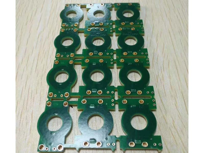
Heavy copper PCB boards ( also being called thick copper board, power board etc ) are usually bonded with a layer of copper foil on a glass epoxy substrate. The thickness of copper foil is usually 18μm, 35μm, 55μm and 70μm. The most commonly used copper foil thickness is 35μm. The thickness of copper foil used in China is generally 35-50μm, and there are also thinner ones such as 10μm and 18μm; and thicker ones such as 70μm. The thickness of the composite copper foil on a substrate with a thickness of 1-3mm is about 35μm; the thickness of the composite copper foil on a substrate with a thickness of less than 1mm is about 18μm, and the thickness of a composite copper foil on a substrate with a thickness of more than 5mm is about 55μm. If the thickness of the copper foil on the PCB is 35μm and the printed line width is 1mm, then for every 10mm length, its resistance value is about 5mΩ, and its inductance is about 4nH. When the di/dt of the digital integrated circuit chip on the PCB is 6mA/ns and the working current is 30mA, the resistance and inductance contained in each 10mm printed line are used to estimate the noise voltage generated by each part of the circuit to be 0.15. mV and 24mV.